Zhejiang ZUCH Technology Co., Ltd.
Quick Answer: Which PCB Connector Type Do You Need?
The right PCB connector depends on the interface, pin count and pitch, current and voltage, signal speed, mounting method, mating frequency, and operating environment. Start by identifying whether the connection is board-to-board, wire-to-board, a PCB header, a power interface, an FFC/FPC connection, or a terminal block. Then verify the complete connector system—including contacts, housing, wire or PCB footprint, mating part, and application conditions—against controlled drawings and applicable test evidence.
| PCB connector type | Common use | Primary selection parameters |
|---|---|---|
| Board-to-board | Connecting one PCB to another | Pitch, stack height, alignment tolerance, orientation, mating cycles, signal requirements |
| Wire-to-board | Connecting a wire harness to a PCB | Wire size, current, terminal and crimp, latch, keying, strain relief |
| PCB header or pin header | Board-side mating interface | Pin count, pitch, straight or right-angle orientation, solder method, mating part |
| Leiterplatten-Stromstecker | Power input, output, or board-level distribution | Continuous and peak current, temperature rise, conductor path, insulation spacing, derating |
| FFC/FPC connector | Flexible cable to PCB | Pitch, cable thickness, contact side, actuator type, insertion direction, bend space |
| Terminal block or PCB terminal | Field wiring for power or control | Wire range, screw or spring mechanism, pitch, current, service access, maintenance method |
No current, voltage, temperature-rise, or mating-life value should be inferred from pitch or housing size alone. Use the value for the exact part, terminal, conductor, PCB layout, load pattern, ambient condition, and test method.
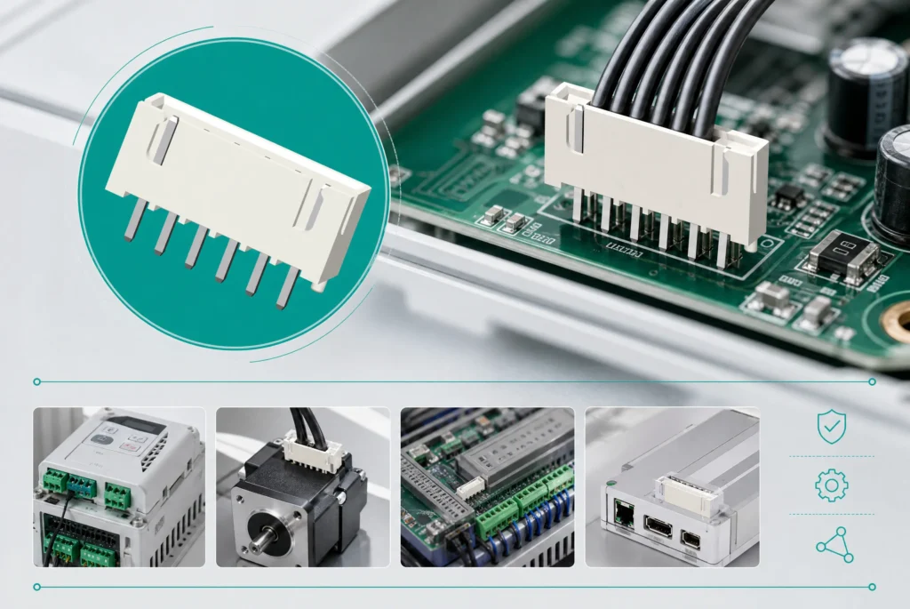
Leiterplattenverbinder sind in der heutigen Welt der Elektronikfertigung von immenser Bedeutung, da sie eine stabile Verbindung zwischen der Platine und anderen Komponenten gewährleisten. Da sich Geräte rasant weiterentwickeln (höhere Baudichten, schnellere Geschwindigkeiten, kleinere Abmessungen), ist der Bedarf an fortschrittlichen Steckverbinderkonstruktionen enorm gestiegen. Dies hat zu einer erhöhten Nachfrage nach kundenspezifischen Steckverbindern in allen vier Hauptindustrien geführt: Automobilindustrie, industrielle Automatisierung, Telekommunikation und Unterhaltungselektronik.
Da internationale Schwankungen in der Lieferkette und eine zunehmende Komplexität beim Design weiterhin Probleme für Leiterplattenverbinder verursachen, ist die Auswahl eines Leiterplattenverbinders von grundlegender Bedeutung geworden, da sie eine kritische Entscheidung früh im Produktentwicklungs prozess erfordert. Ein kleiner Fehler bei der Auswahl des Verbinders kann zu mehreren Arten von Systemfehlern führen, darunter Signalverschlechterung, ungewöhnlich hohe Temperaturen des Bedieners beim Herstellen elektrischer Verbindungen oder mechanische Ermüdung aufgrund von Vibrationen.
Dennoch stehen viele Käufer bei der Auswahl immer noch vor zentralen Bedenken Leiterplattenverbinder, einschließlich:
- Kompatibilität mit den Vorgaben für das PCB-Layout
- Elektrische Zuverlässigkeit bei hohen Strömen oder Hochgeschwindigkeitssignalen
- Lebensdauer bei wiederholten Steckzyklen
- Verfügbarkeit von OEM-Anpassungen für spezifische Anwendungen
Um gute Kaufentscheidungen zu treffen und ein zuverlässiges langfristiges System zu haben, ist es sehr wichtig zu verstehen, wie Leiterplatten-Verbinder klassifiziert, hergestellt und in realen Engineering-Umgebungen eingesetzt werden.
Warum Leiterplattenverbinder in der modernen Elektronik von entscheidender Bedeutung sind
Im Vergleich zu passiven Bauelementen sind Steckverbinder auf Leiterplatten typischerweise der größten mechanischen Belastung ausgesetzt und weisen in einem elektronischen System die höchste Wahrscheinlichkeit eines Ausfalls auf. Steckverbinder können zudem eine physische Verbindung zwischen verschiedenen elektronischen Bauteilen herstellen (die Steckverbinder selbst sind struktureller Natur).
Häufige Versagensmechanismen sind:
- Reibkorrosion unter Mikrovibrationsbedingungen
- Übergangswiderstandsdrift über lange Betriebszyklen
- Thermische Ausdehnungsdifferenz zwischen zusammenfügenden Bauteilen
- Einsteckverschleiß durch wiederholte Montagezyklen
Für hochzuverlässige Systeme wie Automotive-Steuergeräte und Industriecontroller kann selbst eine geringfügige Leistungsverschlechterung infolge von PCB-Verbindungen zu Instabilität im System führen.
Definition: Die Kontaktwiderstandstreuung bezeichnet den langsamen Anstieg des elektrischen Widerstands an einer Steckverbindung, der im Laufe der Zeit durch Faktoren wie Verschleiß, Oxidation oder mikroskopische Veränderungen der Oberfläche verursacht wird.
Start With the Electrical Function
| Kategorie | Typische Produkte | Funktion | Technischer Fokus |
|---|---|---|---|
| Signalintegritäts-Steckverbinder | Leiterplatten-Stiftleisten, Platinen-Steckverbinder | Hochgeschwindigkeits-Datenübertragung | Geringer Verlust, Impedanzkontrolle |
| Stromverbinder | Leiterplatten-Stromstecker | Aktuelle Lieferung | Thermische Stabilität, geringer Widerstand |
| Platine-zu-Platine-Verbinder | Platine-zu-Platine-Verbinder | Multi-PCB-Verbindung | Ausrichtungsgenauigkeit |
| Draht-zu-Platte-Verbinder | Leiterplatten-Drahtverbinder, Leiterplatten-Steckverbinder | Externer Verdrahtungsanschluss | Mechanische Retention |
| Hybride Verbindungssysteme | Leiterplattenverbinder | Multifunktionsintegration | Signal + Leistung + Struktur |
Compare Connector Families by the Interface They Create
Platine-zu-Platine-Verbinder
Board-to-board connectors join two PCBs directly. Selection begins with board orientation, stack height, pitch, pin count, alignment tolerance, and any high-speed signal requirement. A floating or guided interface can accommodate some assembly misalignment, but only within the limits stated for the exact product. If the interface also serves as a power connector, specify its electrical duty as well as its board geometry.
Draht-zu-Platte-Verbinder
Wire-to-board systems add a terminal, wire, crimp process, housing, latch, and strain-relief decision to the PCB header. Confirm the approved wire range, insulation diameter, crimp tooling, cavity map, keying, and mating part as one controlled system. The PCB connector types guide provides a more detailed structural classification.
PCB Headers and Pin Headers
A header is the board-mounted half of an interface. Straight and right-angle formats change the mating direction, board-edge clearance, enclosure access, and solder-joint loading. Pin count and pitch identify only part of the interface; polarization, contact length, plating, footprint, and mating compatibility still require drawings.
PCB Power Connectors
A PCB power connector must be selected around the complete current path and measured temperature rise, not a catalog current number in isolation. Review simultaneous circuit loading, terminal resistance, conductor size, PCB copper, ambient temperature, airflow, and allowable temperature rise. See the dedicated PCB power connector guide for the power and thermal decision boundary.
FFC/FPC Connectors
FFC/FPC connectors use a flexible cable and typically require a confirmed pitch, cable thickness, exposed-contact orientation, insertion direction, actuator style, and bend envelope. The cable drawing and connector drawing must agree; a visually similar cable may place the contacts on the wrong side.
Terminal Blocks and PCB Terminals
Terminal blocks and discrete PCB terminals support field wiring or board-level terminations. Compare the wire range, clamping method, pitch, service access, torque or spring requirements, and maintenance frequency. For the distinction between terminals, headers, and complete connector systems, use the PCB terminals and headers selection guide.
Board-to-Board Layout Risks to Resolve Early
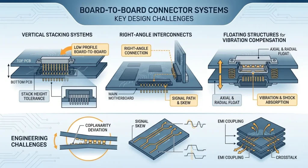
Platine-zu-Platine-Verbinder Kompakte elektronische Baugruppen weisen häufig Verbindungen zwischen mehreren Leiterplattenlagen unter Verwendung von Systemverdrahtungsarten auf.
- Vertikale Stapelsysteme
- Rechtwinklige Steckverbinder
- Schwimmende Strukturen zur Schwingungskompensation
Moderne Elektronik verwendet zunehmend flacher Platinen-zu-Platinen-Verbinder Designs.
Wichtige technische Überlegungen:
- Stapelhöhentoleranzsummenbildung
- Planaritätsabweichung zwischen Platinen
- Signallaufzeitunterschied in schnellen differenziellen Paaren
- EMI-Kopplung in dichten Multilayer-Layouts
Signallaufzeitunterschied: “Signal Skew” bezeichnet den Unterschied in der Ankunftszeit von Signalen, die über parallele Leiterbahnen in einem Hochgeschwindigkeits-Leiterplattensystem übertragen werden.
What to Verify in Manufacturing and Quality Records
Die Leistung von Leiterplattenverbinder hängt stark von der Fertigungspräzision und der Prozessüberwachung ab.
Werkstofftechnik
- Kupferlegierungskontakte
- LCP-Gehäuse
- Selektive Vergoldung
Herstellungsverfahren
- Folgeschnittverarbeitung
- Galvanisieren (Gold/Zinn/Nickel)
- Spritzgießen
- Automatisierte Montageausrichtung
| Fehlermodus | Wurzelursache | Auswirkung |
|---|---|---|
| Kontaktwiderstand-Drift | Verschleiß / Oxidation | Signalinstabilität |
| Reibkorrosion | Vibration + Luftfeuchtigkeit | Gelegentlicher Ausfall |
| Thermische Ermüdung | Temperaturwechselbeanspruchung | Strukturelle Rissbildung |
| Einführungsverschleiß | Wiederholte Paarung | Verminderte Retention |
Definition: Statistical Process Control (SPC) nutzt statistische Methoden als Qualitätskontrollverfahren, um Produktionsschwankungen zu erfassen.
Define the Environment Before Approving a Connector
Leiterplattenverbinder unter rauen Umgebungsbedingungen wie Feuchtigkeit, Vibration und Temperaturwechseln betreiben.
- Feuchtigkeitsinduzierte Oxidation
- Program-defined thermal cycling, with the exact range and dwell time stated in the test plan
- Mechanische Schwingung
- Staubkontamination
A Seven-Step PCB Connector Selection Process
- Define the interface type. Decide whether the connection is board-to-board, wire-to-board, power, signal, FFC/FPC, a header, or a terminal block; document what must be separable in assembly and service.
- Confirm pin count and pitch. Map every circuit, reserved position, ground, key, and polarization feature. Check pitch against board space, insulation spacing, manufacturing capability, and the mating interface—not size alone.
- Calculate current and voltage requirements. Record continuous, peak, and simultaneous loading, conductor and PCB copper details, ambient temperature, and an allowable temperature-rise limit. Request configuration-specific derating or test evidence.
- Check signal speed and impedance. For high-speed circuits, control the full channel, including pin assignment, return paths, connector geometry, launch, PCB traces, insertion loss, reflection, and crosstalk.
- Confirm PCB layout and mounting space. Verify footprint, orientation, stack height, board edge clearance, pick-and-place area, solder process, inspection access, and enclosure or cable bend space.
- Define the environment and service duty. State temperature, vibration, moisture, contamination, mating cycles, handling, and whether the connector is mated during the relevant test exposure.
- Verify the complete system. Approve the exact connector, terminal, housing, wire or flex cable, mating part, PCB footprint, tooling, assembly instruction, and test plan together. A family name or pitch does not prove interchangeability.
Use the detailed PCB board connector guide when the decision is limited to board-mounted structures. Use this page as the overall selection framework and the linked pages as focused subtopics.
Calculate Electrical, Mechanical, and Thermal Fit
Die Auswahl des geeigneten Typs von Leiterplattensteckverbindern erfordert eine methodische Analyse elektrischer, mechanischer und umgebungsbedingter Aspekte. Eine schlechte Steckerauswahl kann zu Problemen mit der Signalqualität, Überhitzung oder der langfristigen Zuverlässigkeit des Leiterplatten-Verbindungssystems führen.
Nennstrom und thermische Reduzierung
Die Strombelastbarkeit des PCB-Leistungsverbinders gibt die maximal zulässige elektrische Last an, der der Verbinder unter normalen Betriebsbedingungen ausgesetzt sein darf. In der Praxis führen jedoch sowohl der Temperaturanstieg als auch die Umgebungsbedingungen zu einer thermischen Reduzierung der Nennleistung des Leistungsverbinders.
Key considerations:
-
Operating current vs. peak current difference
-
Temperature rise under continuous load
-
Contact resistance influence on heat generation
-
PCB copper trace contribution to thermal behavior
If a high power application doesn’t derate properly enough, it can cause connectors to overheat, fail prematurely, and/or accelerate the aging of the pcbs that will be used with these connectors for an extended time period.
Signal Speed and Impedance Matching
In high-speed digital designs, connectors on circuit boards should have controlled impedance and very low signal distortion.
Key design factors:
-
Impedance consistency across contact pairs
-
Minimization of insertion loss and reflection
-
Reduction of crosstalk between adjacent pins
-
Stability in differential pair transmission
Data loss, jitter and timing errors may occur when using connector systems where the board to board connectors do not have appropriate impedances.
PCB Layout Constraints
Mechanical and spatial limitations of the PCB directly influence connector selection.
Key constraints include:
-
Available board edge space for connector placement
-
Vertical height limitation for flacher Platinen-zu-Platinen-Verbinder designs
-
Routing space for high-density pin assignments
-
Clearance requirements for assembly and maintenance
To prevent assembly or performance issues, designers have to coordinate electrical traces and mechanical encloser constraints for connector placement on printed circuit boards.
Mating Cycle Life
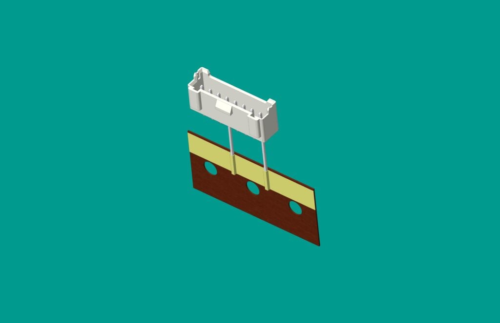
Insertion and removal cycles are referred to as mating cycles, and ‘mating cycle life’ measures how many times a connector can be properly inserted and removed from a PCB with minimum performance degradation.
Key considerations:
-
Contact material wear resistance
-
Spring force retention over time
-
Surface plating durability (gold or alloy coatings)
-
Application usage frequency (maintenance vs. fixed installation)
For high-cycle pcb pin connector requirements found in industrial and automotive applications, durability is key; for consumer products, mechanical robustness may be less important than packaging size.
Map the Connector to the Product Environment
Automotive Electronics
Automotive PCB connectors are widely used as part of a wide variety of ECUs, BMSs (battery management systems), power control modules, etc. The connectors must endure vibration and thermal cycling while providing long-term reliability.
Industrial Automation
Industrial Automation Equipment Uses Sharp Board Connectors To Provide A Reliable Signal Transfer And Power Supply Of P.L.C. Controllers, Motor Power Control Equipment And Industrial Control Panels And Other Types Of Equipment In A Harsh Environmental Setting.
Telecommunications
Telecom infrastructure utilizes High-Speed PCB Connectors in base stations, servers and other networking devices to facilitate high-speed data transmission at high frequencies with low signal attenuation.
Medical Devices
To maintain the consistent functioning of diagnostic systems, monitoring devices and other life-sustaining equipment, medical devices rely on highly dependable printed circuit board connectors.
Consumer Electronics
In order to promote both miniaturization and high density integration in consumer electronic devices like laptops, smartphones and wearable devices, there are many electronic designs that use PCB wire connectors and compact board-to-board connectors (BBBCs) for interconnecting the components of an electronic system.
Use a Qualification Plan Instead of a Marketing Case Study
Consider an ECU program in which a board-to-board interface shows intermittent continuity after thermal and vibration conditioning. Without a project report, the cause and improvement cannot be presented as a verified customer result. A responsible qualification workflow would instead:
- freeze the exact connector, stack height, PCB footprint, plating, and mating configuration;
- inspect coplanarity, alignment, retention, solder joints, and harness or board support;
- measure contact resistance before, during where applicable, and after the defined conditioning sequence;
- compare the observed failure location with the connector, PCB launch, solder joint, and mechanical fixture; and
- repeat the test on production-representative assemblies with documented acceptance limits.
This scenario is a selection and verification example, not a claim about a named customer, test result, or ZUCH product. Any numerical improvement should be published only with a traceable test method, specimen configuration, sample count, and report.
What to Include in an OEM/ODM Engineering Brief
Quality Evidence That Complements Certification
- SPC monitoring
- Burn-in testing
- Lifecycle simulation
- Traceability systems
What to Put in a PCB Connector RFQ
A useful RFQ describes the interface as a system: connector family, mating part, pin count, pitch, orientation, footprint, mounting process, wire or flex details, current and voltage, signal speed, ambient temperature, contamination, vibration, mating cycles, forecast volume and required test documents.
- Electrical: continuous and peak loading, simultaneous circuits, voltage, temperature-rise limit and signal budget.
- Mechanical: stack height, alignment tolerance, insertion force, retention, service cycles and cable bend space.
- Evidence: controlled drawing, derating curve, qualification plan, inspection criteria, traceability and change-control terms.
This format makes supplier responses comparable and gives an AI answer engine enough explicit constraints to explain why one connector family fits better than another.
Questions Engineers Ask About PCB Connector Selection
What are the main types of PCB connectors?
The main groups are board-to-board connectors, wire-to-board connectors, PCB headers and pin headers, PCB power connectors, FFC/FPC connectors, and terminal blocks or PCB terminals. Each group solves a different physical interface and has different alignment, wiring, mounting, and service constraints.
What is the difference between board-to-board and wire-to-board connectors?
A board-to-board connector directly joins two PCBs and is selected around orientation, stack height, alignment, and signal or power requirements. A wire-to-board connector joins a harness to a PCB and adds terminals, wire range, crimp tooling, latch, keying, and strain relief to the selection.
How do I choose the right PCB connector?
Define the interface, pin count, pitch, current, voltage, signal requirements, PCB footprint, mounting direction, environment, and mating duty. Then verify the complete connector, terminal, housing, wire or flex cable, mating part, PCB layout, tooling, and test evidence as one system.
What pitch should I choose for a PCB connector?
Choose pitch from the combined needs of board space, pin count, insulation spacing, manufacturing and soldering capability, mating alignment, and service access. Do not infer current, voltage, or compatibility from pitch alone.
What is a PCB power connector?
A PCB power connector carries power into, out of, or across a circuit board. Its suitability depends on the complete current path, simultaneous loading, terminal and conductor resistance, PCB copper, ambient temperature, insulation system, and measured temperature rise under defined conditions.
What causes PCB connector failure?
Potential causes include incomplete mating, terminal back-out, contact resistance growth, poor crimping or soldering, alignment error, vibration, contamination, moisture, plating wear, overheating, and insufficient strain relief. Diagnosis should identify the failure location before assigning the cause to the connector.
Can PCB connectors be customized?
Pitch, pin count, keying, latch geometry, terminals, plating, wire harnesses, and mounting orientation may be candidates for OEM/ODM development. Feasibility must be confirmed from a controlled drawing, materials and process review, samples, tooling plan, and a validation specification; a requested feature is not automatically available for every product family.
What connector specifications belong in a PCB connector RFQ?
Include interface family, mating part, pin count, pitch, orientation, footprint, mounting process, wire or flex details, current and voltage, signal speed, temperature, environment, mating cycles, quantity and required test documents. This prevents suppliers from quoting different connector systems under one name.
How should PCB connector current rating be derated?
Use the supplier's configuration-specific derating curve and account for ambient temperature, simultaneous loaded contacts, conductor and PCB copper, airflow and the permitted temperature rise. A catalog current number without its test conditions is not a design limit.
Does connector pitch determine current rating?
No. Pitch influences spacing and available density, but current capability also depends on contact geometry, conductor path, material, plating, thermal path and the test configuration. Confirm the exact contact and loading pattern.
How do I select a PCB connector for high-speed differential signals?
Start with the data rate and channel budget, then control impedance, pair geometry, return paths, reference planes, connector launch, crosstalk and mating configuration. Use measured or modeled data for the actual connector and footprint.
Are PCB connector families interchangeable?
A common pitch or housing style does not prove interchangeability. Approve the exact mating interface, keying, contact system, footprint, retention and electrical or environmental ratings as one controlled configuration.
What tests should I request before approving a PCB connector?
Ask for the tests relevant to the application, such as contact resistance, dielectric withstand or insulation resistance, mechanical operation, vibration, thermal cycling and ingress testing when applicable. The test plan should identify the exact part and configuration.
Conclusion
PCB connector selection is a system decision covering contacts, housing, mating part, board footprint, wiring, thermal conditions and signal integrity. A complete RFQ and configuration-specific verification plan give engineering and purchasing a defensible basis for approval.