PCB Header Coplanarity and Solder Reliability in Automated Assembly
An open solder joint at the end of a header row does not, by itself, prove that the connector arrived with bent leads. A lifted termination, a bowed PCB, an uneven paste deposit or tilted placement can produce a similar result. Raising the reflow temperature before distinguishing these causes risks changing a qualified process without resolving the gap. The useful question is where the geometry or solder-contact condition first departed from its approved state: in the loose connector, on the bare board, after printing and placement, or during heating. That distinction determines whether the next action belongs with incoming quality, the connector supplier, the PCB supplier or the assembly team.
The short answer is that PCB header coplanarity must be controlled against the connector drawing, but it is only one contributor to solder quality. Measure unmounted parts independently of the PCB, then compare board flatness, actual paste deposits and placed-component seating before changing reflow. There is no universal coplanarity tolerance: the limit, datum and measurement condition must suit the selected header and validated assembly process. J-STD-001 and IPC-A-610 address soldered assemblies and their acceptability; neither a catalogue listing nor a finished-joint photograph establishes a loose-component dimensional limit. Keep the agreed limit, packaging and incoming check under control, not just the reflow profile.
For a related technical topic, see PCB Header Pitch Selection: Matching Current, Density and Assembly Process.
Contents
What does coplanarity tell you about solder quality?
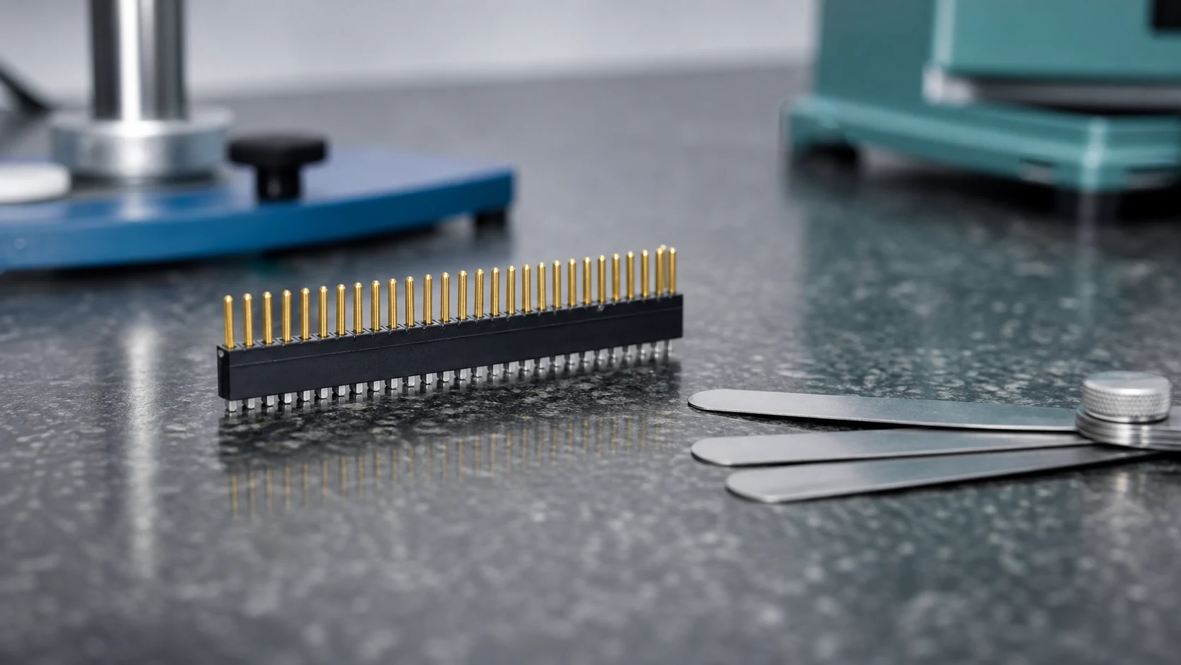
Coplanarity describes how far individual leads or solder surfaces deviate from a common seating plane. A lifted lead may bridge the paste gap poorly or not at all, so the deviation budget contributes to open-joint and weak-joint risk in automated soldering. It does not independently establish solderability, adequate paste volume or acceptable wetting.
For a surface-mount header, identify the solder-contact surfaces and the datum specified on the drawing. Do not substitute the top of the housing or a PCB surface for that datum without an agreed method. For through-hole headers, pin location, insertion depth and seating require their own checks; an SMT lead-to-paste explanation should not be applied unchanged. The drawing also needs to state whether measurement applies as received, after a specified conditioning operation or after thermal exposure.
| Control point |
Question to settle |
Owner |
| Specification |
Limit value and datum definition |
Design and supplier jointly |
| Verification |
Method, sample plan, records |
Incoming quality |
| Preservation |
Packaging and handling rules |
Supplier and logistics |
How can you distinguish a lifted lead from an assembly defect?
Typical signatures are opens or starved fillets on lifted leads, inconsistent joint shapes along one row, or headers that rock on the board before soldering. These are investigation triggers rather than unique diagnoses. A visually acceptable joint also does not establish lifetime under thermal or mechanical stress; application-specific validation remains separate from production inspection.
What should be checked before changing the reflow profile?
- Isolate the connector. Retain suspect loose parts, untouched parts from the same package and a conforming comparison lot. Measure lead heights independently of the PCB using the approved drawing datum. Record which lead is high; a whole-row average can hide an individual outlier.
- Isolate the board. Check the bare PCB’s local flatness at the connector footprint with the agreed support condition. If the defect appears only during heating, compare cold geometry with suitable thermal-warpage evidence under representative support and temperature conditions. A room-temperature measurement after cooling cannot exclude temporary hot warpage.
- Inspect the printed and placed states. Check actual paste height, volume and registration, stencil condition and aperture configuration, then nozzle contact, placement alignment, seating and board support. Compare the pad pattern and connector seating requirements with the supplier drawing and the approved PCB design. Nominal stencil thickness alone does not prove that each pad received the intended deposit.
- Run a controlled comparison. Keep the board lot, paste, stencil, placement setup and profile fixed when comparing suspect and conforming connector lots. Then change only the suspected factor, with a retained baseline and documented inspection criteria. Record connector lot, board lot, lead position and defect result so a disappearing symptom is not mistaken for an identified cause.
If conforming loose connectors fail only on particular boards, prioritize board and assembly checks rather than relaxing the connector limit. If the same lead is out of limit before assembly across independent measurements, contain the connector lot and engage the supplier. Reflow changes become a justified trial only after geometry and deposited-paste checks are documented; verify the measured profile against the component and paste process constraints, and revalidate affected joints before release.
Which design and packaging features preserve lead geometry?
Moulded lead alignment, robust lead geometry and suitable tray or tape packaging can reduce deformation between moulding and placement. Review how the parts are carried, separated and presented to the machine, because handling can alter geometry even when the supplier’s outgoing measurements were acceptable.
Check that the approved pocket or tray restrains the component without loading exposed leads, that removal does not catch a termination, and that the feeder and pickup arrangement match the supplied orientation. Treat packaging changes as controlled changes, not purchasing substitutions. A useful preservation trial compares lead measurements before packing, after the agreed transport simulation or actual shipment, and after unpacking and feeder presentation; it should use the same method and retain package and lot identity.
How should incoming inspection measure and disposition a lot?
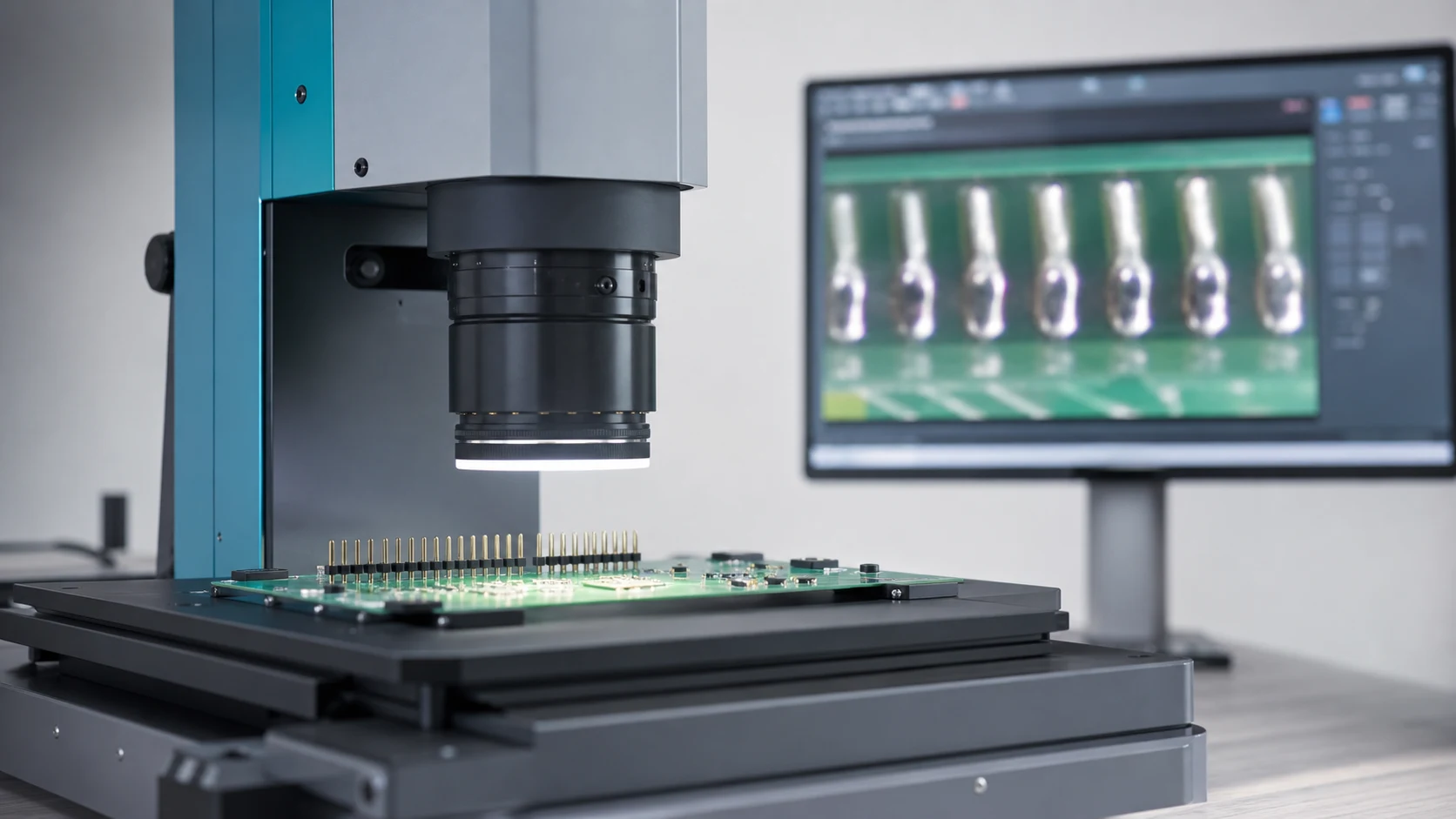
Agree the measurement method, datum plane, sample plan and limit with the supplier, whether the check uses a flat reference plate or an optical system. Keep the method identical on both sides so results can be compared without dispute. Measure the loose connector without force that flattens the leads; document fixture contact, part orientation, instrument resolution, calibration status and repeatability.
Use a written decision rule for results near the limit, including how measurement uncertainty is handled. A borderline result should trigger the approved retest or review route, not repeated measurement until a passing value appears. Retain the original result, identify the retest specimen and method, and hold the affected lot until the authorized disposition is recorded. Passing dimensional inspection does not override an assembly defect or missing process qualification.
| Defect signature |
Possible cause to distinguish |
First response |
| Opens on one row |
Lifted leads, tilted seating or local board bow |
Re-measure loose-part coplanarity, then compare board flatness and placed seating |
| Starved fillets |
Marginal lead height over paste, inadequate deposit or wetting issue |
Review measured lead height against actual paste deposits; investigate wetting separately |
| Rocking part |
Bent leads from handling, seating interference or uneven PCB |
Check on the approved datum, then audit packaging, board support and presentation |
When is lead straightening an acceptable rework action?
Manual straightening of bent leads can work-harden the bend, damage plating or leave geometry outside the intended condition. Define which deviations may be reworked, by whom and with what re-inspection, and route the rest through nonconformance disposition. A lead that looks straight is not sufficient evidence that its solder surface and mechanical condition are acceptable.
Authorize rework only against a documented supplier or engineering instruction for the affected part. Keep reworked parts identifiable, record the operation and remeasure against the unchanged drawing limit. Determine whether additional plating, solderability or assembly verification is needed for that operation; geometry alone cannot show that an altered surface will wet correctly. Do not release an entire lot because a few manually corrected pieces solder successfully.
Important: General guidance cannot approve a specific design or lot. The official IPC revision table below verifies document names and revisions, not detailed acceptance clauses. Apply the selected documents through the controlled drawing, contractual requirements and approved acceptance plan.
What evidence should buyers require before production release?
Close the PCB header coplanarity limit, measurement method, packaging specification, process capability expectations and the reaction plan for violations. Put these in the quality agreement so volume production inherits the controls. Capability claims should identify the measured characteristic, sample population, production conditions and measurement system rather than supplying an unexplained index.
A release record should connect the approved drawing revision to incoming results, packaging-preservation evidence and a representative assembly trial. Include the paste and stencil setup, placement and support conditions, measured thermal profile, joint-inspection criteria, deviations and their dispositions. Agree who can release a held lot and what must be retested after a packaging, tooling, material or process change. Compare the total burden of sorting, retesting, rework and disrupted production, not only the unit purchase price.
Which IPC documents address different parts of the process?
The official IPC Standards Revision Table, checked on October 10, 2026, lists J-STD-001 Revision J (April 2024), Requirements for Soldered Electrical and Electronic Assemblies, separately from IPC-A-610 Revision J (March 2024), Acceptability of Electronic Assemblies. The first concerns soldered-assembly requirements; the second concerns assembly acceptability. Choose the applicable contractual revision and acceptance class before judging finished joints rather than assuming every programme uses the same criteria.
The same table separately lists IPC-7525 Revision C (November 2021), Guidelines for Stencil Design, and IPC-7530 Revision B (January 2025), Guidelines for Temperature Profiling for Mass Soldering Processes (Wave and Reflow). These are relevant to the stencil and thermal-profile branches of fault isolation, not interchangeable with connector dimensional specifications. Only the public revision catalogue was consulted here, not the normative documents; no clause, universal paste allowance or coplanarity threshold is claimed. Obtain the controlled documents and supplier limits needed for the actual process.
What should an assembly-quality inquiry to ZUCH include?
Use ZUCH’s innovation route and the live product catalogue to identify relevant connector, terminal or housing component families. These are discovery routes only and do not demonstrate that a specific configuration is approved for your application.
Which RFQ inputs make the requirement testable?
- Coplanarity limit, datum definition and measurement method, tied to the requested drawing revision.
- Packaging specification and handling rules through placement, including the intended feeder presentation.
- Process capability evidence and inspection records format, with lot identity and measurement conditions.
- Nonconformance reaction plan and rework boundaries, including borderline retests and release authority.
What cannot be approved from this guide alone?
This guide supports engineering and sourcing discussion; it cannot replace programme-specific validation, market requirements, or an approval record. Use ZUCH’s sample request route or contact page for controlled component documentation and samples.

FAQ
What does coplanarity mean for a PCB header?
It is the deviation of lead solder surfaces from the specified common seating plane. For an SMT header, that geometry affects contact with paste, but adequate solderability, board geometry and process control are still required.
How much coplanarity deviation is acceptable?
The limit is design and process specific; agree a numeric limit with the supplier and assembler instead of assuming a generic value. State the drawing datum, measurement condition and decision rule together with the limit.
What solder defects does poor coplanarity cause?
Lifted leads can contribute to opens and starved or inconsistent fillets. Those symptoms are not proof of a connector defect: isolate loose-part geometry from board bow, deposits, placement and wetting before assigning the cause.
How is coplanarity measured at incoming inspection?
Against an agreed datum using a reference-plate or optical method, with a documented sample plan shared with the supplier. Measure unmounted parts without flattening them, retain individual results and follow the agreed review route for borderline values.
Can bent header leads be straightened and used?
Only within an authorized rework instruction and subsequent acceptance plan. Uncontrolled straightening can alter geometry and plating; remeasurement alone may not address every consequence of the operation.
Does packaging really influence coplanarity?
Yes, packaging and extraction can impose loads on exposed leads. Verify preservation with before-and-after measurements through the agreed shipping and machine-presentation conditions rather than accepting a tray or tape format as proof by itself.
What coplanarity topics belong in an RFQ?
Limit and datum, measurement method, packaging, capability evidence, records and the reaction plan for violations. Include retest and release authority, plus the evidence needed when a supplier changes packaging or manufacturing conditions.
References
The four relevant documents below are listed separately in the same official revision catalogue. That source confirms titles and revision dates; it does not provide the full requirements or authorize acceptance limits.
- J-STD-001, Requirements for Soldered Electrical and Electronic Assemblies, Revision J, April 2024 – soldered-assembly requirements; official revision listing.
- IPC-A-610, Acceptability of Electronic Assemblies, Revision J, March 2024 – assembly acceptability; official revision listing.
- IPC-7525, Guidelines for Stencil Design, Revision C, November 2021 – stencil design; official revision listing.
- IPC-7530, Guidelines for Temperature Profiling for Mass Soldering Processes (Wave and Reflow), Revision B, January 2025 – temperature profiling; official revision listing.
What evidence justifies releasing the next header lot?
Reliable soldering starts with distinguishing a component requirement from an assembly outcome. An open joint is a reason to investigate, not permission to widen the drawing limit or increase heat. First establish PCB header coplanarity on unmounted parts, then separate cold board geometry from thermal warpage and examine the actual paste and placed seating. Use controlled comparisons to identify the cause, preserve failed results through retest, and release only against the agreed dimensional and assembly criteria. Packaging and handling evidence must show that accepted geometry survives to placement; a supplier’s outgoing report alone cannot establish that. ZUCH’s catalogue and documentation inquiry routes provide a starting point for discussing a specific configuration, while approval remains dependent on its controlled drawing, representative process trial and recorded disposition.
 Zhejiang ZUCH Technology Co., Ltd.