Treat the connector footprint, mating geometry, reference path, and intended signaling as one design review. Use the drawing, operating conditions, and validation plan before comparing component options.
Contents
Part 1. What signal-integrity risks change with a small pitch connector?
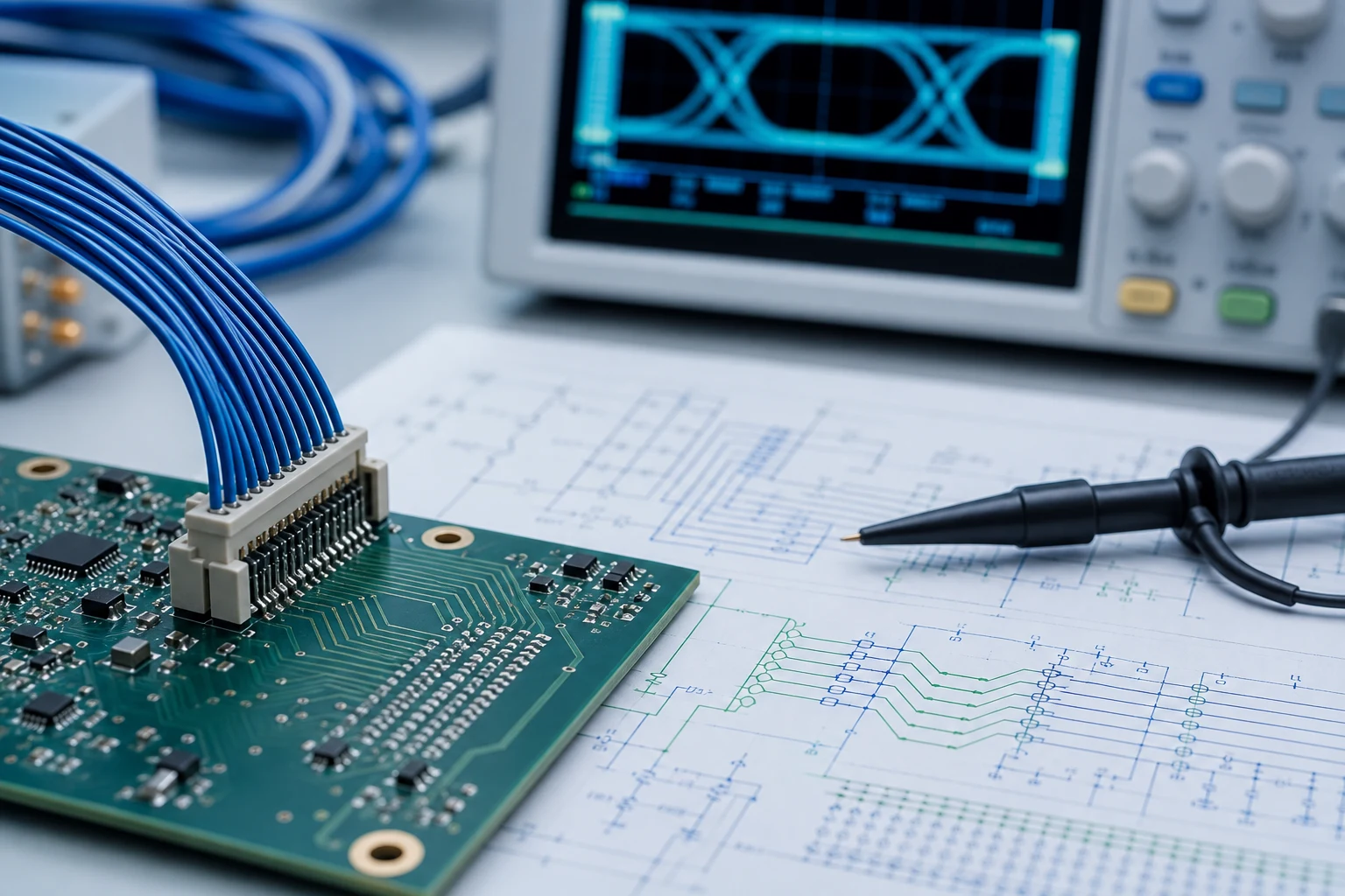
Small pitch does not automatically create a signal-integrity failure. It reduces available geometry and tolerance margin, so the connector, PCB launch, return path, cable or flex transition, and intended data rate need to be reviewed as one interconnect system. A part number alone cannot define that system.
| Review area |
Buyer needs to define |
Why it matters |
| Mating interface |
Both halves, orientation, and operating condition |
Prevents an incomplete component comparison |
| Electrical behavior |
Signal or durability conditions and acceptance basis |
Keeps claims tied to the actual system |
| Mechanical envelope |
Board, enclosure, cable, and access constraints |
Reveals installation conflict before release |
| Evidence |
Samples, drawings, test plan, and change control |
Makes supplier responses comparable |
Part 2. How should the interface and return path be defined?
Map every signal, reference, shield, unused position, and power contact at the interface. A fast signal needs a planned return path through the connector and adjacent PCB structures. Record pin assignment, ground placement, layer transition, and any cable-shield treatment in the controlled drawing.
Part 3. Where do impedance discontinuities and crosstalk begin?
Discontinuities can occur at the board launch, pad/via geometry, contact transition, cable breakout, or a change in return path. Crosstalk risk rises when aggressors and victims run closely without a defined reference strategy. Treat simulations and measurements as design-specific evidence, not a generic connector promise.

| Review input |
Question for engineering |
RFQ output |
| Interface geometry |
What must stay aligned or controlled? |
Drawing and mating-half definition |
| Environment |
What exposure and handling apply? |
Conditions and protection boundary |
| Validation |
What must be demonstrated? |
Sample, method, and acceptance plan |
Part 4. Why do stack-up and launch geometry matter?
The PCB stack-up establishes trace impedance and reference spacing before the connector is installed. The connector footprint, antipad, via stub approach, and breakout routing should be reviewed with the actual board fabricator and signal budget. Do not copy a footprint or trace rule from an unrelated board.
Part 5. How should test access and manufacturing variation be planned?
A design that only works in an ideal layout can be difficult to validate in production. Define probe points or a measurement fixture, connector mating condition, cable state, calibration/de-embedding approach where needed, and the build variations that must be represented in a sample review.
Important: General connector guidance cannot approve a particular finished design. This is a source-note application of the TE and IPC references listed below; define the project-specific method, samples, and acceptance criteria.
Part 6. What belongs in a pre-release validation plan?
The release plan should name the interface, operating condition, measurement method, pass/fail criteria, samples, and change triggers. Review mechanical retention and mating separately from electrical behavior; both can alter the final system result.
Part 7. Which ZUCH product route supports a controlled inquiry?
Use ZUCH’s Small Pitch Connectors route and the live product catalogue to identify a possible component family. These are discovery routes only; they do not prove a specific interface is qualified for the final product.
RFQ inputs
- Controlled mating-interface, drawing revision, and application condition.
- Electrical, mechanical, environmental, and service constraints.
- Required samples, drawings, validation method, and acceptance criteria.
- Required production, traceability, and change-control evidence.
Fit Boundary
This guide supports a structured engineering and sourcing discussion. It cannot replace programme-specific qualification, regulatory review, or an approved validation record. Send controlled inputs through ZUCH’s sample request route or contact page.

FAQ
What is signal integrity in a connector?
It is the ability of the interconnect system to preserve the required signal behavior within the design’s defined limits. The connector, board launch, routing, cable, and return path all contribute.
Do small pitch connectors always have signal-integrity problems?
No. Risk depends on the full interface geometry, signal edge rate, reference strategy, routing, and validation plan rather than pitch alone.
How does crosstalk affect a small pitch interface?
Closely coupled conductors can transfer unwanted energy between signals. Pin assignment, return contacts, routing, and connector/board geometry must be reviewed together.
Why is the return path important?
A signal current needs a defined return path. A disrupted or poorly controlled path can increase impedance discontinuity, noise, and measurement uncertainty.
Can a PCB footprint determine connector performance?
The footprint is one part of the interface. It must be reviewed with the stack-up, launch, connector, cable or flex transition, and application requirements.
What should be measured during validation?
Use the project’s defined measurements, conditions, samples, and acceptance limits. The correct method depends on the interface and intended signaling.
What should be included in a small pitch connector RFQ?
Include the mating interface, pin assignment, PCB stack-up/footprint inputs, signal conditions, environmental and mechanical needs, required drawings, samples, validation evidence, and change-control rules.
References
 Zhejiang ZUCH Technology Co., Ltd.